sábado, 20 de marzo de 2010


Photovoltaic on-demand high voltage pulse generator as an on-board power source for electrostatic actuator array
Jeong B. Lee a, Mark G. Allen b, and Ajeet Rohatgi ba Department of Electrical and Computer EngineeringLouisiana State UniversityBaton Rouge, Louisiana 70803-5901
b School of Electrical and Computer EngineeringGeorgia Institute of TechnologyAtlanta, Georgia 30332-0250
ABSTRACT
The use of amorphous silicon solar cell array high voltage power source as an on-demand wireless power source for electrostatically actuated 32x32 micromirror array is presented. The amorphous silicon solar cell array has been reported previously by authors of this paper1-4. In this work, the solar cell array has been used to drive distributed electrostatic actuator array (micromirror array in this particular paper). A 32x32 micromirror array has been fabricated and the size of single micromirror is 200 m x 200 m. Static deflection test of micromirrors has been carried out and pull-in voltage of 44 V and releasing voltage of 30V was found. The electrical output of the solar cell array has been directly connected to the 32x32 micromirror array to demonstrate a wireless powered distributed MEMS actuator array. A total solar cell array area of 0.3 cm2 (30 series-interconnected solar cells) were used to drive a part of 32x32 micromirror array (a total array area of 0.4 cm2). Motion of multiple numbers of micromirrors was reproducibly observed. The ultimate goal of this research is to achieve power-integrated autonomous MEMS using solar cell array as a miniaturized wireless on-board power source and distributed actuator array as a locomotive engine.
Keywords: Photovoltaic (PV), amorphous silicon, solar cell array, micromirror array, autonomous MEMS, wireless power
1. INTRODUCTION
Regardless of which transducer driving principles are employed, the power requirements of MEMS devices can be quite different from those of general electrical circuitry, therefore requiring either an external power source or additional power conversion circuitry. For autonomous MEMS systems, such as microrobots and space-based MEMS, self-contained on-board or remote (i.e., wireless) power sources are desirable. Though the importance of the problem, work focusing either on wireless or on-board power sources for MEMS devices/systems or power-integrated MEMS systems are rare. One of the previous works in this area is a series-interconnected array of 100 single solar cells (amorphous silicon solar cells) reported by the authors of this paper1-4. In the previous work, we reported a series interconnected array of 100 single amorphous silicon solar cells in an array area of 1 cm2 in an integrated fashion, and produces an array open circuit voltage of 150 V with a short circuit current of 2.8 A. Another very promising work in wireless transmission of energy is from Sasaya et al5. They reported an in-pipe wireless micro robot based on wireless energy supply by TE11 mode of microwave.
In this paper, the use of solar cell array high voltage power source as an on-demand wireless power source for distributed electrostatic MEMS actuator array (in particular, a 32x32 electrostatically-actuated micromirror array) is presented. This paper consists of a brief reintroduction of solar cell array and discussion of ultimate goal of the research, design issues and fabrication of 32x32 micromirror array, characterization and modeling of micromirrors, and demonstration of power-integrated MEMS which combines photovoltaic (PV) wireless on-demand power source and the 32x32 micromirror array as an example of a distributed actuator array.
Corresspondence: J. B. Lee; Email:
jblee@ee.lsu.edu; Telephone: 225-388-5621; Fax: 225-388-5200; Homepage: http://www.ee.lsu.edu/jblee.
2. PHOTOVOLTAIC TECHNOLOGY AS A WIRELESS POWER SOURCE FOR ELECTROSTATIC/PIEZOELECTRIC AUTONOMOUS MEMS SYSTEMS
The power requirements of MEMS devices depend mainly on the driving principles involved. Several driving principles that are suitable in the micro-domain are used to drive MEMS devices. The most common driving principles include electrostatic drive, piezoelectric drive, electromagnetic drive, and electrothermal drive. Typical power requirements for each driving principle are shown in Table 1 below. Regardless of which transducer driving principles are employed, the power requirements of MEMS devices can be quite different from those of general electrical circuitry, therefore requiring either an external power source or additional power conversion circuitry. Of the common driving principles, electrostatically- and piezoelectrically-driven MEMS devices need relatively high voltage ranging from tens of volts to hundreds of volts with the current in the range of nA~A. In many cases of laboratory-level experiments, external high voltage power source is commonly used for powering electrostatically- and piezoelectrically-driven MEMS devices (see Figure 1).
Table 1. Typical power requirements of MEMS devices.


Figure 1. Schematic representation of common methods of powering MEMS.
Previous investigations1-4 from authors of this paper proposed a series-interconnected array of 100 single solar cells (amorphous silicon solar cells) in a total array area of 1 cm2 as a wireless power source for MEMS. The solar cell array was fabricated in an integrated fashion to produce an array open circuit voltage (Voc) of 150 V, and an array short circuit current (Isc) of 2.8 A under air mass (AM) 1.5 conditions. Such a high voltage output in miniaturized size has strong potential to be used as wireless power sources for autonomous MEMS systems. The ultimate goal of the research is to realize a constant high voltage PV power source (100 V or higher) with on-demand high voltage MOS (metal oxide semiconductor) switching circuitry which is controllable by on-demand external electrical signals (3.3 V or 5 V level). Figure 2 shows a schematic diagram of an on-demand high voltage switching circuitry with constant high voltage PV power source, which uses a combination of high voltage PV power source and high voltage MOS switching circuitry. When high voltage MOS switch is turned on output voltage would be low (near 0 V) and when high voltage MOS switch is turned off high voltage (~100 V) would be delivered to individual MEMS devices.

(a) (b)Figure 2. (a) A schematic diagram of power-integrated autonomous MEMS; (b) a schematic block diagram of the power module.As an initial step of the realization of such a power integrated autonomous MEMS, a simple optically modulated on-demand PV power source has been used to actuate multiple numbers of actuator array using electrostatically-driven micromirror array that is described in the following section.
3. A 32x32 MICROMIRROR ARRAY
A 32 by 32 micromirror array built in this work is similar to Texas Instruments Digital Mirror Device (DMD)6, but has several different approaches with the goal of enabling low cost manufacturing. The micromirror arrays have been built on low cost substrates, such as glass, instead of relatively expensive CMOS-processed underlying circuitry. Such an approach allows the realization of relatively low cost, passive micromirror array elements. Approaches taken in this work for the fabrication of micromachined mirror arrays include a line addressing scheme7, a seamless array design for high fill factor, planarization techniques of polymeric interlayers8, a high yield methodology for the removal of sacrificial polymeric interlayers, and low temperature and chemically safe fabrication techniques.
3.1. Design
Figure 3 shows a schematic drawing of a single micromirror. The square-shaped micromirror is suspended at its center by thin and narrow hinges, which are supported at their ends by electroplated nickel posts. A higher fill factor results in higher perceived resolution, yielding more natural images. The micromirror designed in this work has the size of 190 m on a side and the width of the hinge is 4 m. The pixel pitch size is 200 m. The fill factor for this micromirror is 83.75 % (33,500 m2 / 40,000 m2). The thickness of the organic sacrificial layer (i.e., the air gap for micromirror actuation) ranges from 18 m to 24 m, resulting in deflection angle ranges from 10.7 to 14.2.


Figure 3. A schematic diagram of a micromachined mirror.
3.2. Finite element modeling for resonant frequencies
Finite element modeling (FEM) of the micromirror was performed using the finite element modeling package ANSYS 5.2 to calculate resonant frequencies and mode shapes. The geometrical parameters used in the FEM are as shown in Table 2. The element type used has eight nodes with six degrees of freedom (DOF) at each node: displacements in nodal x, y, and z directions and rotations about nodal x, y, and z-axes. Since the hinge is the area of interest for torsional behavior of the micromirror, hinges and adjacent areas were densely meshed while most of the plate was coarsely meshed.
Table 2. Parameters used in FEM for resonant frequencies of the micromirror.Young’s modulus of Al 70 GPaPoisson ratio of Al 0.33Density of Al 2710 kg/m3
Figure 4 (a), (b), and (c) show the first three mode shapes. Resonant frequency data for the first six modes are shown in Table 3. The fundamental mode resonant frequency is 6.5 kHz which is the determining factor for the switching speed of the micromirror. Since this micromirror array uses a line addressing scheme, the minimum time field for one frame is 4.96 ms (153 s * 32 = 4.9 ms). If the micromirror array works as a black & white display (no gray scale), then the maximum frame rate would be as high as 204 Hz (1/4.9 ms).

Figure 4. Resonant mode shapes of the micromirror: (a) fundamental mode; (b) second mode; (s) third mode.Table 3. Finite element modeling results for modal analysis of the micromirror.Mode Natural Frequency [Hz]1 65312 158763 195294 413515 800036 83985
3.3. Fabrication of micromirror array
A brief fabrication procedure is shown in Figure 5. Fabrication of micromirror arrays started with 3 inch by 2 inch glass substrates. Evaporated Ti/Au (thickness of 300 / 4,000 Å) row addressing lines were patterned using the liftoff process. A BCB layer was spin-coated to planarize the patterned metallic lines. A silicon dioxide (SiO2) passivation layer was deposited using PECVD to protect the BCB layer during the very last step of dry etching for bonding pad opening. Evaporated Ti/Au (300 / 4,000 Å) column addressing lines (also serving as an electroplating seed layer for posts) were patterned using the liftoff process. Two different organic interlayers, both single and double coats of PI 2611, were spin coated as polymeric sacrificial layers. In the case of a single coat of PI 2611, the coated layer was soft baked at 150 C for 30 minutes. The thickness of the soft-baked single coat of PI 2611 layer was approximately 18 m. In the case of a double coat of PI 2611, samples were soft baked after each spin at 120 C for 20 minutes and hard baked at 300 C for one hour in nitrogen ambient after the second coat. The double-coated PI 2611 thickness was approximately 24 m.
A 1,000 Å aluminum hard mask was prepared for via cutting by the liftoff process. Reactive ion etching (incident power of 300 W, pressure of 300 mTorr or less, oxygen gas flow rate of 50 sccm) was used to define 10 m by 10 m square via holes. Etch rate was about 0.25 m/min. for hard cured PI 2611, and 0.6 m/min. for soft cured PI 2611. After via cut, the aluminum hard mask was removed by diluted hydrofluoric acid (HF) which was followed by nickel (Ni) electroplating. After the Ni electroplating, the surface of the polyimide electroplating mold and plated Ni had roughness of about less than 1 m. A 7,000 Å aluminum layer was then deposited using DC sputtering and patterned to form hinge and micromirror plate structures. Finally, the organic sacrificial layer was etched away by an isotropic dry etch using a barrel plasma etcher. Figure 6 show SEM photomicrographs of a side view of the corner of the completely released 32 by 32 micromirror array and a closeup view of the electroplated nickel post and the Ti/Au seed layer. The organic interlayer was safely and completely removed and left overhanging micromirror array structures. The gap between micromirror plates and the planarization BCB layer is 18 m, which allows 10.8° angular deflection. Figure 7 show SEM photomicrographs of top views of a part of micromirror array and a single micromirror after the completion of organic interlayer etch.


Figure 5. Fabrication procedures for micromachined mirror actuators on low cost substrates.


Figure 6. SEM photomicrographs of completely released 32 by 32 micromirror array.

Figure 7. SEM photomicrographs of top views of a part of the micromirror array after the completion of organic interlayer etch.3.4. Micromirror actuation and static deflection modeling
The completely released micromirror array was placed on an optical microscope and the gap between the micromirror and planarized BCB/SiO¬2 layer was measured to be 18 m. The deflection of the tip of the micromirror was measured by focusing on the tip of the micromirror using a Nikon MM-11 Measurescope and measuring the deflection of the microscope head necessary to keep the deflecting tip in focus. The displacement characteristic (deflection versus applied voltage) is shown in Figure 8 (a). The measured pull-in voltage (Vp) is 44 V, and the releasing voltage (Vr) is approximately 30V.


Figure 8. Displacement characteristic of the micromirror.
Theoretical modeling for the static deflection of the micromirror was performed with several assumptions and those results are compared with the measurement results. Figure 9 shows the schematic drawing of a cross section of a micromirror used for the theoretical modeling. When an external voltage is applied between the grounded micromirror and the address electrode, a potential energy W is stored in the system. The electrostatic force which acts normal to the substrate is complex since there is a fringing effect, and the direction of the electrostatic force changes as the micromirror rotates. Simple theoretical models, however, may be established with following assumptions: (1) the hinge is straight, of uniform rectangular cross section, and of homogeneous isotropic material; (2) the hinge is loaded only by equal and opposite twisting couples, which are applied at its ends in planes normal to its axis; (3) the hinge is not stressed beyond the elastic limit; (4) the fringing electric field is negligible. In reality, the fringing effect should not be neglected, but this assumption was made for this simple theoretical model. Figure 9 and Table 4 shows the material properties and geometrical parameters used in the theoretical modeling.
Table 4. Material properties and geometrical parameters used in theoretical modeling.Material Properties Geometrical ParametersYoung’s modulus of Al 70 GPa Z0 18 mPoisson ratio of Al 0.33 Z1 2.5 mShear modulus of Al 26.3 GPa Z2 0.5 mDensity of Al 2710 kg/m3 t 0.7 m w 4 mRelative permittivity of BCB 2.7 a 190 mRelative permittivity of SiO2 3.9 b 190 m L 60 m
The mechanical torque Tm is defined as follows: , (1)where k is the torsional spring constant,  is the deflected angle in radians, G is the shear modulus of elasticity, Ip is the polar moment of inertia, and L is the length of the hinge. The shear modulus of elasticity G is defined as follows: , (2)where E is the Young’s modulus, and  is the Poisson ratio.


(b)Figure 9. A schematic drawing of a single micromirror: (a) top view and a closeup of the hinge; (b) cross section of a micromirror.
When the aspect ratio (thickness/width) is lower than 1 (1 = square cross section), a theoretical expression for the polar moment of inertia (Ip) is given9 as follows: . (3)At the maximum deflection (=10.8=0.1885 rad), the mechanical torque Tm turned out to be 3.3622*10-11 [N-m] based on equation (3). The electrostatic torque Tel can be represented as the following expression: , (4)where Wel is the electrostatic energy stored in the system, V is the applied voltage, C is the capacitance of the system. Since the rotation angle for this micromirror is small (between 0 and 10.8), the tangent of  could be assumed equal to . The maximum error due to this assumption is 1.2 %. The analytical solution for the electrostatic torque Tel is calculated using Mathematica. The Taylor expansion of the analytical solution about =0 is: (5)
The first term is same as the parallel plate capacitor case. Higher order terms correct for the fact that the capacitance and torque change nonlinearly as the micromirror rotates. Figure 8 (b) shows the theoretical model for the attraction cycle of the micromirror compared with the measurement data. The discrepancy is within 39 %. The discrepancy between the measurement data and the theoretical model for the attraction cycle of the static deflection characteristics of the micromirror could be due to a combination of several causes. In our case, the aspect ratio of hinge is approximately 0.175 (0.7 m/4 m), so the tensile residual stress of 0.79 GPa (which is approximately 1 % of the Young's modulus of aluminum) can increase the required voltage for pull-in to the measured value of 44 V. The second important cause could be measurement errors in the geometrical parameters of the hinge of the micromirror. If there is a 10 % measurement error in the thickness of the hinge, then the polar moment of inertia changes 33.1 %, and subsequently the required voltage changes 15.4 %. A combination of these two causes and other minor causes may make the 39 % discrepancy between the measurement data and the theoretical model.
4. A PHOTOVOLTAIC POWER-INTEGRATED MICROSYSTEM(A WIRELESS POWERED MICROMIRROR ARRAY)
The 32 by 32 micromirror array was connected to the output of the series interconnected solar cell array to demonstrate a power integrated MEMS actuator array (see Figure 10). Since the micromirror requires 44 V for full deflection, only 30 series-connected cells (total array area of 0.3 cm2) under air mass (AM) 1.5 illumination were required to drive the micromirror array. It should be noted that the size of the micromirror array (array area of 32x32 micromirrors is 0.4 cm2) is about the same size of the wireless photovoltaic MEMS power source (0.3 cm2). Based on this size comparison, it can be claimed that photovoltaic technology could be suitable wireless on-board power source technologies for certain (such as electrostatic/piezoelectric) MEMS systems.


Figure 10. A schematic representation of a wireless powered micromirror array.
The fabricated 32 by 32 micromirror array was placed on a probe station (Signatone S-1160A-6N) and directly connected to the output of a photovoltaic power (amorphous silicon solar cell array) through probes (Signatone S-725). The device was observed using an optical microscope with video camera, connected to a display monitor and a video cassette recorder (VCR). Motion of single micromirrors as well as a part of the micromirror array could be reproducibly observed and video recorded. Light modulation at the light source has been successfully used to turn the multiple numbers of pixels (micromirrors) on and off. Figure 11 shows optical micrographs of a part of the micromirror array, undeflected (a), and several pixels at right of array energized and deflected (b), respectively.
Figure 11. Optical micrographs of a part of micromirror array: (a) undeflected; (b) several pixels at right of array energized and deflected.
ACKNOWLEDGEMENTS
Material donations from Dow Chemical are greatly appreciated. Microfabrication, except as noted below, was carried out at the Georgia Tech Microelectronics Research Center. The support of the staff of the Pettit Microelectronics Research Center at Georgia Tech is acknowledged. The amorphous silicon deposition was carried out at Solarex, Inc. The secretarial support of the staff of the Department of Electrical and Computer Engineering at Louisiana State University is acknowledged.
REFERENCES
1. Jeong B. Lee, “On-Board Power Supply and Remote Driving Mechanisms for MEMS”, in IEEE/CRC Industrial Electronics Handbook, (CRC Press, Boca Raton, FL), Chapter 119, pp. 1538~1546, May 1997.2. Jeong B. Lee, Z. Chen, M. G. Allen, A. Rohatgi, and R. Arya, “A Miniaturized High Voltage Solar Cell Array As An Electrostatic MEMS Power Supply,” IEEE/ASME Journal of Microelectromechanical Systems, vol. 4, no. 3, pp. 102~108, Sep. 1995.3. Jeong B. Lee, Z. Chen, M. G. Allen, and A. Rohatgi, “A Hybrid Micro System Using a High Voltage Solar Cell Array as a Power Supply,” in 1994 International Symposium on Microelectronics, Boston, MA, (SPIE Vol.2369), pp. 438~443, Nov. 1994.4. Jeong B. Lee, Z. Chen, M. G. Allen, A. Rohatgi, and R. Arya, “A High Voltage Solar Cell Array As An Electrostatic MEMS Power Supply,” in Proceedings 7th IEEE Workshop on Micro Electro Mechanical Systems, Oiso, Japan, pp. 331~336, Jan. 1994.5. T. Sasaya, T. Shibata, N. Kawahara, “In-Pipe Ireless Micro Robot,” in Digest of Technical Papers of 10th International Conference on Solid-State Sensors and Actuators (Transducers ’99), Sendai, Japan, pp. 1058~1061, Jun. 1999.6. L. J. Hornbeck, “Deformable-mirror spatial light modulators,” in Proc. of the SPIE - The International Society for Optical Engineering, SPIE vol. 1150, pp. 86-102, 19907. V. P. Jaecklin, C. Linder, N. F. De Rooij, J. M. Moret, and R. Vuilleumier, “Line-addressible torsional micromirrors for light modulator arrays,” Sensors and Actuators A, vol. 41-42, pp. 324-329, 19948. Jeong B. Lee, J. English, C. H. Ahn, and M. G. Allen, "Planarization Techniques for Vertically Integrated Metallic MEMS on Silicon Foundry Circuits," Journal of Micromechanics and Microengineering, vol. 7, no. 2, pp. 44~54, June 19979. Roark, “Formulas for stress and strain,” McGraw-Hill, p. 349.
FRANCO RIVERA
CRF
Nanosatellite Communication and MEMS Technology

Nick Pohlman, Jeremy Opperer and Patrick Schubel
Department of Mechanical Engineering Northwestern UniversityEvanston, IL 60208
Project Summary This paper explores the growing segments for potential use of MEMS devices. In particular, we focus on space-based applications in which MEMS have yet to play a significant role. If the performance of particular MEMS devices can match those of macro-sized components, the same system objectives can be achieved while significantly reducing the overall weight – usually the driving factor in spacecraft design. Of course, modifications in spacecraft architecture will hopefully evolve as MEMS components prove their performance in the space environment. Examples are given for future distributed satellite missions showing that a greater quantity of smaller satellites with individualized capabilities can help reduce production cost as well as add robustness to the entire mission. Control of position and velocity are natural requirements of the distributed architecture. In order to trade sensor information effectively, remote communication must play a key role. Therefore, the remainder of this report focuses on MEMS RF communication devices. Examples of phase shifters, signal filters, switches and antennas are given. The modeled performance of the switch and antenna are derived as well as the processes used for fabrication. Finally, an example is given of a MEMS RF-switch tested in orbit. The results indicate that MEMS structures can be cheaper to place in orbit and achieve improved performance over macro-sized devices.Keywords: MEMS, RF Communication, satellites, space-based communication systems, MEMS fabrication processes, MEMS modeling
Introduction When NASA Administrator Daniel Goldin introduced the new catch phrase, “Faster, Better, Cheaper” he may not have envisioned where spacecraft technology would head over the next decade. The defining parameter in most spacecraft is payload weight for launching from the earth’s surface to outer space [1, 2]. As expected there is a direct relationship between launch cost and vehicle weight. If the overall system weight can be lowered, or distributed, the potential for reducing satellite launching costs can be significantly improved. Naturally, the development of Micro-Electro-Mechanical Systems (MEMS) has expanded into the space sector. By cutting the mass of components onboard the space vehicle, the launch costs and hopefully the overall budget for production can be reduced. Furthermore, other features of MEMS devices, aside from their small size, can benefit system components, such as power. By converting from solid-state electronics to mechanical systems, the power consumption of a device can be significantly lowered. This increase in efficiency could help reduce the battery power, size, and charge necessary to operate the satellite. Similarly, solar panel sizes could be smaller again bringing down the overall mass and power consumption of the satellite. Two key advantages arise when considering MEMS devices in space applications. The first advantage is realized by lowering launch cost. Currently, launching a spacecraft into low Earth orbit (LEO) costs about $10,000 per kilogram, and placing a craft into a higher geosynchronous Earth orbit (GEO) costs about $50,000 per kilogram [3]. Obviously, by reducing mass, designers stand to gain in reducing total project cost. The second advantage is the devices’ resistance to radiation and vibration. Cosmic radiation can upset the operation of solid state components, but MEMS structures can withstand radiation. In addition, because MEMS devices have such a low mass, potentially damaging inertial and vibration forces are minimized. A rocket launch can induce very high accelerations, but with a robust MEMS design the possibility of damage is low [4]. Nanosatellites, roughly classified as satellites weighing 1-10 kg, are some of the most promising spacecraft being designed today. Below 1 kg, satellites are classified as picosatellites. MEMS can revolutionize their design when applied to the communications, data processing, navigation, and propulsion systems.
Satellite Missions and MEMS: Past, Present and Future One must consider what scientific objectives could be accomplished on such a small platform. One of the driving factors of programs such as NASA’s New Millennium Program (NMP) is distributing satellite capability and costs across separate vehicles rather than placing all focus on a single, monolithic device. In shrinking the size, the cost of replacing a damaged or failed component can be drastically altered. Budgets for failed single satellite missions have cost billions of dollars without any capability for rectifying the problem. Two missions that can be compared and contrasted are the Hubble Space Telescope, and the Chandra X-Ray Observatory [5]. Hubble’s original failures due to an out of focus lens have been well documented. Fortunately, with a significant investment in time and manpower, the problem was fixed thereby allowing the space telescope to operate with its original purpose. It is interesting to note that the entire Chandra X-Ray Observatory Satellite project was nearly cancelled due to worries of similar problems experienced with Hubble. With an orbital perigee of approximately 6,000 statute miles, Chandra is well beyond the orbital range that can be reached by the Space Shuttle. Conversely, Hubble, with a closer orbit of only 350 miles could be reached and repaired by a human crew. Any component failure aboard Chandra, from mirror lenses having a speck of dust or a failed switch on the camera, could have caused the $1.5 billion project to be a complete failure without any means to rectify. If either of these satellite systems could have been distributed over a network of smaller satellites, the potential repair (and possibly production) costs could be more reasonable for a successful space mission. Hopefully with the added robustness of distributed satellite systems, NASA and other space agencies can avoid budget catastrophes such as those experienced with the Mars Surveyor in 1999. One outcome from initial NMP research has shown that Formation Flying of multiple satellites can help distribute the single satellite payload capability. Many future NASA and military missions are basing their design on such capabilities, for example the Terrestrial Planet Finder [6] and TechSat 21 [7] shown in figure 1. By expanding the number of satellites in a formation to more than one, the total aperture size can be increased allowing for improved resolution without adding cost for connecting the components with structural hardware. Without a rigid connection, the relative motions of payload components must be maintained with tight navigation and control tolerances. Previous missions such as Earth Observing 1 have shown the capability to maintain relative orbital motion or to conduct autonomous maneuvers with standard solid state electronic hardware and macro-size propulsion and control systems [8]. These types of proof of concept experiments are even planned for microsatellite missions. Future NASA missions like Space Technology 5 & 6 (figure 2) hope to be one of the first satellites to use actual MEMS devices in design and production [9]. The Air Force and DARPA are supporting expansion into miniaturization with their University Nanosatellite Program [10]. While some microsatellites will use standard components, with one component necessary for the entire mission payload, the overall size of these satellites will begin to decrease in size, making MEMS more important features for spacecraft production.


Satellite Systems System components can roughly be segregated into three major categories: propulsion, navigation and communication. Micro-thrusters have been explored to help reduce the size of propulsion components on the vehicle making attitude control cheaper by using smaller devices and less fuel. Furthermore, navigational aids such as GPS receivers and gyroscopes are able to reduce the overall size of the navigation payload with MEMS technology. Another important aspect that must be included in all motion control is feedback from sensors. Naturally on a monolithic satellite, each component will be directly hardwired to an overall communication bus allowing information to be exchanged quickly. The new architecture of distributing satellite capabilities across a fleet of separated vehicles presents a new problem for overall communication design. With the new architecture, reliable and adaptable communication systems are going to need to be developed for remote communication between devices. Algorithms and communication standards are being developed and shared to enhance capabilities of remote satellites not only with the ground, but also amongst their own fleet [11]. For example, if only one satellite in a multi-vehicle fleet has a star sensor to determine orientation, it must communicate the measurement to the other members of the fleet in order for all pieces to move as a cohesive unit. Autonomous capability to reconfigure networks and remote communication will be necessary for fleets to maintain continuity for operation. Occlusions to communication could happen as satellites cross paths or distances become too large. Potentially, some satellites’ primary purpose would be simple relays of information between vehicles separated over too great a distance. If the remote communication devices were based on MEMS technologies, many different communication capabilities could be carried on a single microsatellite allowing for potential to overcome single-point failure or allow the overall system to re-configure relatively easily. The remainder of this report will not explore the details of specific communication protocol or information, which are generally mission specific, but rather indicate devices that have potential in space applications for remote communication between separated vehicles.Nanosatellite Communication Systems and MEMS The communication system on any satellite consists of two basic mechanisms: a transmitter and a receiver. Satellites usually deal with signals in the microwave range, which are high frequency, short wavelength signals that can carry a large amount of information. Often, the signals are in the gigahertz (109 Hz) radio frequency (RF) range. In order to effectively transmit and receive RF signals, satellites must have extremely sensitive signal processing equipment. Also, the signal must be able to transmit over a large distance with very high fidelity and fast data rate. Currently, most microwave signal handling is done with solid-state electronic components. Electrical performance of microwave components is determined almost entirely by the mechanical dimensions of the devices, and precision in the manufacturing of these components is extremely important [12]. MEMS devices are very attractive to use in these applications in this respect because of the ability to accurately control their dimensions. The design of conventional solid-state microwave and RF devices is hindered by three constraints, which are power consumption, sensitivity, and size [13]. MEMS can improve on conventional designs in all three of these areas, as well as offering a lower production cost. As frequencies are driven higher and higher by increased data transmission requirements, the shortcomings of conventional designs are compounded by the lethargic response of macro-sized components [14]. Also, in an increasingly crowded radio spectrum, high sensitivity is crucial. By integrating a MEMS device directly on a silicon chip and semiconductor circuit, energy consumption and signal noise are reduced even further. MEMS devices in a nanosatellite can be used as signal filters, micro-switches, and antenna components such as phase shifters. Some examples of each of these components will be presented as well as some of the fabrication and performance parameters.
Signal Filters An RF circuit requires at least one filter to pull out a desired signal from a receiving antenna or to insert one to be transmitted. Currently, surface acoustic wave (SAW) filters are used to do this job. However, these filters are relatively large and do not work well at very high frequencies [13]. Digital signal processing can be done on the back-end of the process, but this consumes valuable electrical power from batteries or solar panels. MEMS designs are well suited to perform front-end analog frequency filtering, taking up less space and using less power because the device is passive. By increasing filter sensitivity, potential exists to improve communications systems. A filter could not only preselect a communications band, but also perform channel selection within that band, enabling significant improvement over existing technology. In one such design, a passive microwave filter is deposited on a GaAs membrane and displays very low power loss and good performance [15]. First, a 2.2 m thick membrane is machined utilizing RIE techniques on the GaAs wafer. To fabricate the filter structure, a 0.7 m gold layer is deposited on the membrane and conventional contact lithography, e-gun evaporation, and lift-off techniques are used (figure 3). This device could easily be coupled with other components such as antennas, capacitors, and inductors on the same substrate.

RF-MEMS switches Switches are vital to the successful operation of an antenna array. They are used for beam shaping and steering by individually selecting elements in the array [16]. Conventional switches suffer from losses in efficiency and have higher insertion losses, due to parasitic effects of the system. MEMS switches, on the other hand, do not suffer from these problems. These switches have properties that are ideal for MEMS space-based applications, including the following: low insertion losses, rapid response, improved power handling, wide bandwidth, good electromagnetic isolation, and high open position isolation. Drawbacks are minor, but include stiction and a comparatively slower response time with active components. Several switch designs have been explored. Cantilever and membrane (bridge) types are the most popular, however there are also seesaw bar, rotary, and derrick-type switches that are available for specialized applications [14]. Selection of the specific design may include parameters such as insertion loss and isolation criteria. For membrane switches, both insertion loss and isolation are a function of the change in capacitance during the on and off states. To decrease the insertion loss, contact should be as close as possible. Conversely, improved isolation requires the conductors be as far from each other as they can in the off position. An electrostatically actuated MEMS coplanar waveguide (CPW) shunt switch is shown in figure 4. It is comprised of a metallic bridge between two off-center pull-down electrodes. A supplied bias voltage moves the bridge into contact with the ground. The in-line configuration of the switch results in a compact design with high isolation at 0.1-18 GHz and specifically, with regard to inductance to ground, the isolation at mm-wavelengths is –20 dB at 18GHz [17]. This can be compared with capacitive contact shunt switches with high isolation ranging between 10 and 120 GHz.

Figure 4. RF-MEMS CPW shunt switch schematic [16] Force balance is used to calculate the electrostatic force as follows, (1)where , A, V, d, and x are the permittivity of the free space, projected area of the electrodes, applied voltage, gap between the line and bridge, and the deflection of the bridge respectively. A restoring force, Fs, is given as (2)
where the spring constant, k, can be found with the following equation, (3)where E, t, w, L, and  are the effective Young’s modulus of the bridge material, thickness, width, and length of the bridge, residual stress, and Poisson’s ratio respectively [16]. If the deflection is greater than 1/3 d, the system becomes unstable and pull-in occurs. The voltage required for this may be calculated by (4) The resonant frequency of the cantilevered beam is another important design consideration. It controls the maximum speed under which the switch can reliably perform. Attenuation also varies as √f. This frequency can be determined by considering the beam to be supported at both ends, where (5)with a given system mass, m. For the aforementioned shunt switch, an attenuation of 0.4 dB/cm occurs at 10 GHz[17]. Given the two states of the MEMS switch, isolation and insertion loss, the following values may be calculated from impedance and capacitance. When in the down-state position, the switch can be modeled as an RsL circuit. Switch resistance, Rs, is defined by half the sum for the resistance at the contact points and at the short transmission line, Rc and Rl respectively. With impedance given as Z0, the isolation can be found with the following equation, (6)The insertion loss for the up-state position can be calculated by modeling the switch with two sections of transmission lines, with two capacitors, to represent switch and electrode coupling, and two bias resistors. Therefore, by using an RC model, the loss can be found by (7)where Cb and Rb are the capacitors and resistors respectively. Trends for the insertion losses for this switch design can be found in figure 5. Here, the strong dependence on bias resistance is shown, while the bias capacitance has a variable effect on the loss [17].
Figuer 5. Calculated insertion loss of the dc-contact shunt switch: (a) variation of loss with Rb for Cb=88fF and (b) variation of loss with Cb for Rb=2400 and 600 [17] The capacitance ratio for the switch in its off and on states can be used as a measure of its performance. These are given by the following two equations: (8) (9)where d and hd are the dielectric constant and height respectively. The isolation ratio can therefore be solved by (10)By examining this equation, one finds the advantages to using a highly dielectric thin film deposition. The addition of a dielectric layer does not affect the pull-down voltage [16]. The manufacturing process for RF MEMS switches (figure 6) is similar to that of many other MEMS devices fabricated by batch lithographic processes. An example of the micromachining process steps can be found in figure 7. The 40 m  20 m dimple reduces contact resistance at each of the contact areas. A 1.7 m PECVD SiO2 layer is grown as a sacrificial layer, as seen in the figure step (c). The dimples are created by partially etching the PECVD layer by about 5500 Å. 0.8 m sputtered Au is used to create the 300 m  100 m bridge. A buffered HF solution is then used to remove the SiO2.
Figure 6. Final cross section of switch [17]
Fig 7. (a)-(f) Process steps of the dc-contact shunt switch with dimple and bias resistor procedures and (g) switch in the down state position. Cross section shown in figure 6 [17] Even with the advantages gained from a MEMS switch, before it can be used in a nanosatellite, the lifetime of the switch will have to be lengthened. In a long-term application such as a deep-space satellite, a lifetime of 100 billion cycles is required. Currently MEMS switches do not have this lifespan [18]. Obviously, the long-term solution to this problem is to improve the material strength or structure design of the switch for increased lifespan. One rapid solution method could be to have additional redundant switches that only operate after failure of a predecessor switch. With the additional space and mass freed by using MEMS components, added redundancies can be included to make entire satellite system more robust.
Antennas This section will now shift focus from individual switch design to another communication component, the RF antenna. General considerations will be introduced followed by specific examples, including a Hilbert Curve Fractal Antenna (HCFA). Planar antennas are important in both the transmission and reception of signals in nanosatellites. With a MEMS-based design, an antenna can be integrated with other passive or active components. Also, many antennas can be arranged on the same substrate, allowing a phased array configuration [19]. In a specific design by IMT-Bucharest, an antenna is fabricated on a 1.5 m thick silicon oxide/silicon nitride dielectric membrane micro-machined from a silicon substrate, called a double-folded slot antenna. Gold is then electrochemically deposited on the wafer to form the antenna of thickness 2.5 m, shown in figure 8. The two cross members of the antenna are placed one half wavelength apart for good radiation performance [19]. The device operates at 77 GHz and could be easily be included in a nanosatellite design. Another design of a MEMS antenna, called a V-antenna (figure 9), has moving parts and can be reconfigured for adaptation in new environments. The arms of the V-shaped antenna can be moved independently with comb drive micro-actuators and a forward- or backward-moving bias. When both arms are moved in the same direction with a fixed angle, the antenna can be used to steer the radiation beam and focus its reception or transmission of data [14]. The shape of the beam can also be adjusted by changing the angle. This technology has been demonstrated for a 17.5 GHz MEMS V-antenna.
Figure 8. Photo of 77 GHz MEMS antenna on dielectric substrate [19]
Figure 9. Top view and details of a reconfigurable 17.5 GHz V-antenna [14]
Phase Shifters Another application where MEMS devices can improve upon current solid-state design is in phase shifters. A phase shifter is a type of phased-array antenna that can be configured to transmit or receive signals in different directions without being physically reoriented. Already extensively used in microwave satellite communication tasks with FET or diode technology, a MEMS design could drastically reduce power loss. A phase shifter works by altering the transmission path of the antenna with an array of switches, providing different amounts of phase modulation of the signal. By using a MEMS switch design, which was covered in detail in a previous section, the existing design could be improved upon while reducing the cost [13]. Because a large amount of research has been done on the design and placement of switches in a phase shifter, a MEMS phase shifter would differ from an existing one only in the fact that the solid state switch is replaced by a MEMS switch [18]. A schematic of a MEMS phase shifter is shown in figure 10.Figure 10. Phase shifter composed of an array of RF-MEMS switches [18]

HCFA Fractal antennas are also employed for MEMS space-based communication. Similar to V-antennas with regard to their incorporation of MEMS devices, fractal systems are capable of adjusting their characteristics to suit specific needs for reconfiguration in changing environments [16]. Hilbert curve fractal antennas (HCFAs) are well suited to satellite broadcasting. These can maximize the amount of space available for RF communication.MEMS technology eliminates the need for the more expensive, bulkier, and less efficient conventional phase shifters. Furthermore, high frequency array batch fabrication can be carried out on a single chip. HCFAs utilize switches and phase shifter as integral parts of their design. Their multiband nature, useful for multiplexing, and size to weight ratios make them much more attractive than their conventional macro-sized counterparts. Design of and experimental results for HCFAs will now be addressed. HCFA take advantage of the relatively self-similar pattern of the fractal, as seen in figure 11. This figure shows 4 iterations of Hilbert curves. The additional line segments used between each iteration are small compared to the overall geometry, and can be considered negligible. For each iteration order, the line length of the segments dramatically grows while the area covered by the antenna footprint increases only moderately. This shows how the curve almost fills the plane. Resonant frequency can be significantly reduced for a given area by increasing the number of iterations, thereby averting a problem many small-scale antennas encounter. This approach is similar to that of Euclidian based geometrical systems; however, the use of fractals can help achieve higher degrees of freedom. Figure 11 provides a more detailed look at the individual segments of the fractal. The total inductance of the system can be calculated by determining the inductance of the turns of the meander line. The inductance of a regular half-wavelength dipole can then be compared to this total inductance.
Figure 11. Generation of four iterations of Hilbert curves [16]
Assuming a constant dipole configuration capacitance, the induction of the system can be calculated with the following equations. First, line segment length, d, can be defined as (11)where l and n are the outer dimension and iteration order of the fractal. The number of short-circuited parallel segments of length d can then be defined by (12)The total length of wire not forming parallel sections can also be defined as (13)Now, the characteristic impedance of the transmission line can be calculated by the following equation, (14)where the diameter, b, and spacing, d, are obtained from the fractal geometry. is the intrinsic impedance of the free space. Input impedance at the end of the line can then be found, (15)The impedance for the straight-line segments is therefore, (16)where there are m sections of input impedance, is the permeability of free space and  is a function of the system. Resonant frequency can be found by equating the total inductance with that of a half-wave dipole, where l=/2 [16]. Since regular dipole antennas have resonance at quarter wavelength multiples, the equation for the first several HCFA resonant frequencies is given as (17)where k is an odd integer. This equation only considers low order effects and is not recommended for high order modes. Figure 12 shows the measured input impedance compared with calculated values for a third iteration fractal antenna at various frequencies. For the corresponding radiation patterns, there are fewer nulls present than would be expected for a dipole antenna due to the smaller overall size of the radiator.
Figure 12. Input impedance of 7x7 cm2 HCFA of third iteration [16]
Reconfigurability of the HCFA is achieved by incorporating RF-MEMS switches in series with the length of the antenna, thereby facilitating frequency tuning. Such agility would be required if ambient operating conditions were to change, altering frequency characteristics. The frequency tuning characteristics of the antenna are shown in figure 13 by the voltage standing wave ratio (VSWR) as a function of the various switching configurations and frequency, when two switches are located at adjacent nodes. Furthermore, radiation patterns are also presented in figure 14. Activating switches to enable additional line segments have generated these patterns. Changes in the xy-plane are provided due to their dominance in the system.
Figure 13. Frequency tuning of HCFA: case 1, both switches closed; case 2, one switch opened; case 3, both switches open [16]

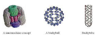
Figure 14. Radiation patterns for HCFA with additional segments, shown in the xy-plane [16]
Table 2. Phase shift in each arm and resulting peak direction of the beam [16]Case Elem. 1 phase Elem. 2 phase Elem. 3 phase Elem. 4 phase Beam dir1 0 0 0 0 0˚2 0 20 40 60 6˚3 0 40 80 120 13˚4 0 60 120 180 19˚5 0 90 180 270 29˚6 0 120 240 360 38˚
Picosatellite Experiment Initial experiments for MEMS components have been conducted with low earth orbit (LEO) satellite payloads. As previously mentioned, cost savings achieved though reducing payload weight can be realized through the use of such technology. A Stanford University designed satellite, the Orbiting Picosatellite Automated Launcher (OPAL), has released multiple picosatellites for testing individual MEMS devices [20]. The Aerospace Corporation with funding from DARPA engineered one of the picosatellites with an array of RF-MEMS switches onboard developed at Rockwell Science Center (RSC) [21]. Specifications of the switches are as follows: low insertion losses at 40GHz of 0.2 dB, isolation >60 dB at dc and ~25 dB at 40 GHz, actuation voltage ~80 V, on/off response within ~10 s, mechanical response reliability (no modulus reduction) after 60 billion cycles, and hot-switched lifetimes 7 orders of magnitude at ~1mA. The RSC microrelay is approximately 250 m  250 m. The microrelay is fabricated in a similar manner as shown in figure 7. The surface micromachining is performed under 250 C. High conductivity evaporated Au is used for all RF signal and dc lines. The sacrificial layer is removed, in this instance, by dry release etching in an oxygen plasma. This small system consumes very little power as a result of its electrostatic actuation. Shifts in the elastic constant resulting from plasma enhances chemical vapor deposition (PECVD) SiO2 are negligible. The switch experiments conducted in the picosats employed four MEMS switches in series with resistances of 3, 10, 30, and 300 k. Batteries rated at 3 V were used to power the satellites, and inductive charge pump circuits were used to generate the 100 V (25% over voltage) for switch activation. On February 6th, 2000, two picosatellites were released from OPAL and began orbiting the earth in a sun-synchronous 750 km polar orbit. A 30.5 m tether was used to maintain a constant separation distance between satellites because they did not have any control thrusters to adjust their relative positions. Each satellite had dimensions of 10.16  7.62  2.54 cm3. The RF MEMS switches were switched on and off repeatedly as requested by programming uploaded from a base station on earth. A standard radio communication and networking module was used to as the means for remote communication. Photographs of the system can be found in figure 15. The picosatellites were only in visible communication range of the base station two times each day for approximately 300-600 seconds during each pass. During such contact, information regarding switching status and temperature would be transmitted. While this picosatellite experiment did not test a complete MEMS communication system, it has shown how individual MEMS devices can be launched and tested in space without significant experimental costs. Indirectly, the mission showed how MEMS communication components would help improve mission robustness in the future. Unfortunately, the picosatellite mission was shortened by nearly 75% while the standard radio modem was broadcasting in the “transmitting” state attempting to form a link to the ground station. The continuous operation of the radio module drained the limited battery supply during the initial stages of the mission. If for future missions, the module is replaced by a MEM system, the power drained from initialization can be reduced allowing longer life for fixed power storage devices.Conclusions and Recommendations There are many opportunities for MEMS communication devices in the space industry. With an increasing emphasis on designing spacecraft with lower mass and cost, MEMS structures are ideally suited for a nanosatellite platform. While these devices can be incorporated in the satellite propulsion and navigation systems, some of the most practical and beneficial applications of MEMS devices exist in the satellite communication system.
The primary obstacles that must still be overcome are proof of operation in space environments and extending the overall lifetime of the equipment. However, MEMS structures have proven to be quite robust under harsh conditions. Due to lack of experience, suggestions for improvements of particular fabrication procedures would be fruitless. Time and future experiments will help determine which fabrication tools are best equipped to withstand environments and requirements for space hardware. One suggestion for overall MEMS space communication would be to form a standard set-up such that all future communication could follow a pattern and devices would be easily interchangeable. This could benefit the space industry as a whole by forming a network of MEMS satellites in a higher orbit. Currently satellites are not capable of continuous communication with a single ground station. Often remote locations must be linked to the main control center through standard landlines such as fiber optics. With a network of MEMS satellites (similar to GPS), one would always have visibility to a single unit thereby allowing a single station to tap into information being shared amongst all of the satellites in the network. Essentially, satellites on the “backside” of the planet could communicate to the sole ground station through the MEMS communication network (i.e. a plethora of information on the world-wide-web, but one computer only taps into one site/satellite of interest). Scientists at the beginning of the 20th century never imagined that their discoveries would facilitate the perpetuation of human space exploration. In much the same, we stand at the cusp of the 21st century with an expanding technology from MEMS devices. Like their gargantuan predecessors, hopefully MEMS will be used to extend humankind’s outreach beyond our planetary bounds thereby extending NASA’s simple credo to “Faster, Better, Cheaper and Smaller!” References1. Judy, J.W., Microelectromechanical systems (MEMS): fabrication, design and applications. Smart Materials & Structures, 2001. 10(6): p. 1115-1134.2. Cass, S., MEMS in Space, in IEEE Spectrum. 2001. p. 56-61.3. Huang, A., et al. A Microengineered Cold Gas Thruster System for a Co-Orbiting Satellite. in MEMS Components and Applications for Industry, Automobiles, Aerospace, and Communication. 2001. San Francisco, USA: SPIE.4. Martin, M. and S. Kilberg, TECHSAT21 and Revolutionizing Space Missions Using Micro-Satellites. 200, USAF http://www.interfacecontrol.com/papers/TechSat21MicroSats.pdf.5. Roy, S., Exploring the Invisible Universe: The Chandra X-ray Observatory. 1999, NASA http://www1.msfc.nasa.gov/NEWSROOM/background/facts/axaf.html.6. Laboratory, N.J.P., Terrestrial Planet Finder. 2002, Nasa http://planetquest.jpl.nasa.gov/TPF/tpf_index.html.7. Directorate, S.V., TechSat 21 Space Missions Using Satellite Clusters. 1998, Air Force Research Laboratory http://www.vs.afrl.af.mil/factsheets/TechSat21.html.8. Young, J., Earth Observing-1. 2002, NASA Goddard Space Flight Center http://eo1.gsfc.nasa.gov/.9. Beck, S., Space Technology 5. 2002, NASA New Millennium Program http://nmp.jpl.nasa.gov/st5/.10. Janni, J.F., Nanosatellites Preparing for Launch. 2000, Air Force Office of Scientific Research http://www.afosr.af.mil/pages/january00.htm.11. Flournoy, D., Online Journal of Space Communication http://satjournal.tcom.ohiou.edu/. 2002, SSPI.12. Fiedziuszko, S.J. Applications of MEMS in Communication Satellites. in Microwaves, Radar and Wireless Communications MIKON-2000. 13th International Conference on,. 2000: IEEE.13. Cass, S., Large Jobs for Little Devices, in IEEE Spectrum. 2001. p. 72-73.14. Lubecke, V.M. and J.-C. Chiao. MEMS Technologies for Enabling High Frequency Communications Circuits. in Telecommunications in Modern Satellite, Cable and Broadcasting Services, 1999. 4th International Conference on. 1999. Nis, Yugoslavia: IEEE.15. Konstantinidis, G., et al. GaAs Membrane Supported Millimeter Wave Filters. in MEMS Components and Applications for Industry, Automobiles, Aerospace, and Communication. 2001. San Francisco, USA: SPIE.16. Vinoy, K.J. and V.K. Varadan, Design of reconfigurable fractal antennas and RF-MEMS for space-based systems. Smart Materials & Structures, 2001. 10(6): p. 1211-1223.17. Tan, G.-L., A DC-Contact MEMS Shunt Switch. IEEE Microwave and Wireless Components Letters, 2002. 12(6): p. 212-214.18. Rebeiz, G.M., G.-L. Tan, and J.S. Hayden, RF MEMS Phase Shifters: Design and Applications, in IEEE Microwave Magazine. 2002. p. 72-76.19. Neculoiu, D., et al. MEMS Antennas for Millimeterwave Applications. in MEMS Components and Applications for Industry, Automobiles, Aerospace, and Communication. 2001. San Francisco, Ca: SPIE.20. Twiggs, R., Orbiting Picosatellite Automatic Launcher. 2001, Stanford University, http://ssdl.stanford.edu/opal/.21. Yao, J.J., et al., Microelectromechanical system radio frequency switches in a picosatellite mission. Smart Materials & Structures, 2001. 10(6): p. 1196-1203. Biography
Patrick Schubel received his BS in mechanical engineering at the University of Dayton in 1999 and MSME from Northwestern University in 2002, where he is now a PhD student. His interest lies in experimental mechanics and composite behavior. His research has included studying the fracture mechanics response of tires and quantifying effects of porosity on the strength of aerospace fiberglass. Besides being a dedicated scholar, he enjoys playing cards, driving his 1990 Mercury Grand Marquis, and rock and roll.

Nick A. Pohlman received a B.S. in Mechanical Engineering from the University of Dayton in 2000 and a S.M. in Aeronautics and Astronautics from the Massachusetts Institute of Technology in 2002. He is currently conducting research and working to complete a Ph.D. in Mechanical Engineering from Northwestern University. His future interests include obtaining tenure at an academic institution and having a guest appearance with Kermit the Frog or a cameo in the next Superman film.

Jeremy G. Opperer received a B.S. in Mechanical Engineering from Lawrence Technological University in 1998 and a M.S. in Mechanical Engineering from Northwestern University in 2002. He is currently conducting top secret research and working to complete a Ph.D. in Mechanical Engineering from Northwestern University. His interests include long walks on the beach and a warm fire to cuddle up to. He also enjoys tennis and the ancient art of the caber toss.


A Brief Overview of Potential Environmental Pollution and Health HazardsResulting from Possible Military Uses of Nanotechnology with Implications for Research Priorities Helpful to Prevent and/or Reduce Such Pollution and Hazards


A nanomachine concept A buckyball Buckytube

Results from a Two-Round Expert Delphi
Conducted by theMillennium Project of the American Council for the United Nations University
for theArmy Environmental Policy Institute
February 2005

The content of this report does not necessarily reflect the views the Millennium Project’s sponsors.
Executive Summary
An expert panel of 29 participants identified potential military uses of nanotechnology that might occur between 2005–2010 and 2010–2025 with their potential for causing health hazards or environmental pollution.
Some examples between 2005 and 2010 are:
• Nanosensors to detect trace concentrations of biochemicals could lead to absorption of nanoparticles through the skin into the body and environment, concentrating in water and soil, and eventually linking with natural organisms, causing unknown environmental changes
• Nanomaterials (e.g., nanotubes) in uniforms and equipment to make them stronger and lighter could lead to nanofiber-like materials that break off from uniforms and equipment and enter the body and environment
• Nanoparticles as surface coverings to make it harder, smoother, and/or more stealthy could erode and be inhaled by military staff and the general population
• Nanomaterials used as filters to remove selected impurities from fluids could become very low in cost and hence ubiquitous, and result in many small but discrete concentrations of possibly toxic impurities.
Some examples between 2010 and 2025 are:
• Artificial blood cells (respirocytes) that dramatically enhance human performance could cause overheating of the body, bio-breakdowns, and their excretion could add to the environmental load.
• Large quantities of smart weapons — especially miniaturized, robotic weapons and intelligent, target-seeking ammunition without reliable remote off-switches could lead to unexpected injury to combatants and civilians, destruction to infrastructure, and environmental pollution.
• Small receptor-enhancers designed to increase alertness and reduce the reaction times of humans could cause addiction and/or subsequent Chronic Fatigue Syndrome, leading to weakness, neural damage, and death. Research Priorities: The expert panel also identified and rated research questions whose answers might produce knowledge to help prevent or reduce the health hazards and environmental pollution from potential military uses of nanotechnology. Those research questions or directions that would produce the most new knowledge to prevent or reduce health hazards (rated 4 or higher on a 5 point scale) are:
• How are nanoparticles absorbed into the body through the skin, lungs, eyes, ears, and alimentary canal?
• Once in the body, can nanoparticles evade natural defenses of humans and other animals? What is the likelihood of immune system recognition of nanomaterials?
• What are the sizes, aspect ratios, and surface activity determinants of nanoparticle impacts on living organisms (research must be conducted for specific nanoparticles)?
• What are potential exposure routes of nanomaterials - both airborne and waterborne?
• Are the current toxicity tests used for chemicals appropriate and/or useful for nanomaterials?
The research directions that would produce the most new knowledge to prevent or reduce environmental pollution from future military use of nanotechnology (rated 4 or higher on a 5 point scale) are:
• How biodegradable are nanotube-based structures?
• Could nanoparticles enter the food chain by getting into bacteria and protozoa and accumulate there?
• How will nanomaterials enter the environment and will they change when moving from one medium (e.g. air) to another (e.g. water)?
• How to identify and dispose of nanomaterial litter?
• How might nanoparticles get into plants and other organisms?
• Regardless of the question, the research should be interdisciplinary and international.
• Do nanoparticles act like bioaccumulants in Nature?
• How can nanotechnology be used for post-battlefield cleanup (including biological, chemical, and nuclear wastes) so that they do not pollute soil and water?
• What technologies can be used to minimize exposure to nanomaterials?
Introduction
A nanometer is one billionth of a meter (10-9 meter). Nanotechnology manipulates matter at this nanoscale. It is more of an approach to engineering than a science, although it draws from the scientific knowledge of biology, physics, chemistry, and materials science and is expected to dramatically change these sciences. See Appendix B for a list of other definitions. Eric Drexler introduced the term “nanotechnology” in Engines of Creation (1986) to describe the “manipulation of individual atoms and molecules to build structures to complex, atomic specifications,” and said that “Perhaps the ‘arrival’ of the concept of nanotechnology came about in physicist Richard Feynman's landmark 1959 lecture called There's Plenty of Room at the Bottom: The principles of physics … do not speak against the possibility of maneuvering things atom by atom … it has not been done because we are too big.”
Today many other kinds of nanotechnology have attracted much attention. Global nanotech investments in 2004 were estimated at $8.6 billion, and revenues from nanotech products should equal that of information technology in ten years. President Bush signed into law the 21st Century Nanotechnology Research and Development Act , providing $3.7 billion beginning in 2005 and spread over four years, as the largest governmental funding of scientific projects since the space program.
The applications of nanotechnology range from next generation flat panel TVs, advanced solar panels, and chemical and biosensors, to nanomedicine and energy transmission efficiencies. Richard Smalley, who discovered the first fullerenes, called “buckyballs (C60), and is developing the use of “buckytubes,” expects nanotech to help improve energy transmission efficiencies. (Buckyballs are the hollow C60 spheres; a fullerene is any pure carbon molecule with 60 or more atoms, e.g. carbon nanotubes.)
Nanotechnology approaches range from “top down” (large machines that make very small things today like nanomaterials in tennis rackets, clothing, and sunscreens) to “bottom up” approaches (molecular assemblers that one day may make molecular machines that make larger things). This study invited input on the full range of approaches to nanotechnology from an expert panel via a two-round Delphi. The invitation letters and Delphi questionnaires are available at:
http://www.acunu.org/millennium/nanotech-rd1.html and http://www.acunu.org/millennium/nanotech-rd2.html.
The 29 expert Delphi panel respondents had backgrounds in nanotechnology R&D with potential military applications, medicine, and/or environmental research related to nanotechnology. This study was conducted between September 2004 and January 2005 as a small addition to a contract with the Army Environmental Policy Institute to produce monthly scanning reports about international environmental security issues.
1. Potential Use and Potential Impacts between 2005 and 2010
The Delphi panel was asked to suggest potential environmental pollution and health hazards that might result from military uses of nanotechnology in the time periods 2005–2010 and 2010–2025.
The following is an unranked list of the panel’s suggestions (edited and condensed for clarity) that might occur between now and 2010:
1. Nanomaterials in sunscreens, camouflage creams, and/or bioweapons skin shields might be absorbed through the skin and/or flushed into the environment and enter the food chain.
2. Nanomaterials in uniforms and equipment to make them stronger, harder, smoother and/or lighter could be damaged and/or through normal usage and aging, break off and enter the body and environment including plants, other animals, water and fish.
3. Nanoparticles in fuel as additives might be inhaled by military staff and the public.
4. Nanoparticles as surface coverings to make it harder, smoother, and/or more stealthy could erode and be inhaled by military staff and the general population
5. Nanosensors to detect trace concentrations of biochemicals could lead to absorption of nanoparticles through the skin into the body and environment, concentrating in water and soil, and eventually linking with natural organisms, causing unknown environmental changes.
6. Very low cost filters/membranes using nanomaterials to remove selected impurities from fluids (liquids and gases) could become ubiquitous and result in many small but discrete concentrations of possibly toxic impurities that could become more toxic than the initial materials.
7. Nanoparticles in weapons such as depleted uranium could be inhaled by military in the battlefield and civilians if dispersed via wind or other means.
8. Similarly, nanoparticles created by the blast of high technology weapons and/or high temperature combustion processes could lead to diseases like cancer, lymphoma, or leukemia in humans and other animals induced by inhalation of nanopollution or ingestion of contaminated food; e.g., inhaled nano-sized pollution in the Twin Towers Collapse Phenomenon.
9. Nanoparticle accelerants and explosives could be accidentally dispersed into the environment.
10. If implanted into the body, radio frequency identification device (RFID) tags to track soldiers and equipment could result in materials "leaching" into the body; those in equipment could enter the environment.
11. More effective prophylactics and therapeutics—e.g. time-released polymers that would replace multiple vaccinations—would give better control over contracting and spread of illness and disease; however, those polymers would end up in the environment.
12. The biocompatibility of improved prosthetic devices (non-friction microscopic coatings) and implanted medical devices has yet to be established.
13. Disposal of highly efficient batteries using nanomaterials could impact ecosystem and human health.

2. Potential Use and Potential Impacts between 2010 and 2025
The following is an unranked list of the panel’s suggestions (edited and condensed for clarity) that might occur between 2010 and 2025:
14. Artificial blood cells (respirocytes) that dramatically enhance human performance could cause overheating of the body, bio-breakdowns, and their excretion could add to the environmental load.
15. Large quantities of smart weapons—especially miniaturized, robotic weapons and intelligent, target-seeking ammunition without reliable remote off-switches could lead to unexpected injury to combatants and civilians, destruction to infrastructure, and environmental pollution.
16. Small receptor-enhancers that increase alertness and reduce the reaction times of humans could cause addiction and/or subsequent Chronic Fatigue Syndrome, leading to weakness, neural damage and death.
17. Inorganic, non-biodegradable nanoparticles (and perhaps also non-biocompatible) nanoparticles for drug release or cancer treatment, or "permanent" nanosensors, might induce a foreign body reaction.
18. Proteomic targeting, genetically selective "designer quasi-viral components", engineered to select specific human targets based on definable genetic markers, might mutate, creating a biological pandemic.
19. Nanoparticles to "clean-up" contaminated areas might create new compounds that could have unknown impacts on the environment, including long-term leaching into ground water reserves.
20. Ubiquitous surveillance systems deployed without strong controls on the use of information could lead to psychological stress from the sense of being watched by strangers.
21. Numerous centimeter-scale buoyant platforms deployed in the atmosphere might interfere with birds and aircraft, and damaged devices might fall as precipitation at uncontrolled locations over Earth's surface.
22. Nanoscale time-released bioweapons for inhalation might have long-term effects on those handling the bodies of victims and on the environment in general.
23. The deliberate high-volume production and use of nano-built weapons and ammunition might occur without sufficient disposal methods after the need for use has passed.
24. Nanaoscale biomolecule-driven motors that enhance the efficiency of ATP (adenosine triphosphate) usage, the frequency of generation of ATP and the life of ATP molecules in endurance athletes and/or long-haul soldiers could cause overheating of the body, bio¬breakdowns, and possibly lead to Rapid-Onset Muscle Soreness after a stipulated duration, and if allowed to function beyond this duration, may kill the organism thus modified.
25. Ubiquitous sensing in the oceans via large numbers of small drifting devices linked by acoustically based data-packet networks, and countermeasures to disable them, could affect sea life from these materials, as well as from acoustic pollution.
Other interesting suggestions for the period 2010 to 2025 that are not conventionally thought of as health or environmental impacts included:
• Nanocomputers could remove humans from the battlefield making warfighting less costly for the side with the nanotechnology and therefore make warfighting more likely. The reduction in lethality of wars aided by nanotechnology could reduce the moral sanctions against wars of aggression. Better sensors, effectors, and computational systems, with lower cost production enables deployment of teleoperated "soldiers" able to occupy territory without risk to human soldiers, could destabilize military balances, prompting preemptive wars or wars of aggression, enabling inexpensive conquest and subsequent suppression of insurgencies, and even a reduction in moral sanctions against wars of aggression. Rapidly deployed high-volume production of superior weapons and ammunition might have similar impacts.
• Automated or remote-controlled weapons, rather than removing humans from the field of battle, instead may make it easier to take the battlefield to the humans. Although these new weapons may shift the focus of conflict away from conventional battlefields, new battlefields will have to be developed, and many of them will overlay civilian populations.
• Inexpensive, high performance military systems make nonlethal weapons economical as a means of projecting force, despite their lower effectiveness per unit cost.
• Antisatellite systems based on inexpensive, high performance launch and orbital systems could lead to dense clouds of hazardous objects in near-Earth space, posing collision threats, strategic destabilization, and precipitating war.
• Special operations nanorobots designed to shoot from the inside, after being ingested, might miss their targets and lead to random killings.
3. Research priorities
3.1 Research priorities for addressing health hazards
The Delphi Panel was also asked to identify and rate research questions, that if pursued might help prevent or reduce environmental and health impacts. The following scale was used to rate the questions:
Potential for gaining new knowledge from the research
5 = Will lead to critical knowledge for preventing and/or reducing problems 4 = Very likely to lead to critical knowledge for preventing and/or reducing problems3 = May lead to critical knowledge for preventing and/or reducing problems2 = Not likely to lead to critical knowledge for preventing and/or reducing problems1 = A complete waste of time
The tables below present the averages of the ratings by the Delphi panel listed in order of their potential for gaining new knowledge important to reducing or preventing potential health impacts noted previously.
Health hazard research questions––sorted by Knowledge Gain PotentialHow are nanoparticles absorbed into the body through the skin, lungs, eyes, ears, and alimentary canal? 4.46Once in the body, can nanoparticles evade natural defenses of humans and other animals? What is the likelihood of immune system recognition of nanomaterials? 4.38What are the sizes, aspect ratios, and surface activity determinants of nanoparticle impacts on living organisms (research must be conducted for specific nanoparticles)? 4.14What are potential exposure routes of nanomaterials - both airborne and waterborne? 4.00Are the current toxicity tests used for chemicals appropriate and/or useful for nanomaterials? 4.00What are the surface properties of nanoparticles that alter toxicity? What are the distinct properties of nanoparticles that may alter toxicity? 3.87Do nanoparticles concentrate at critical sites like synapses and tumors? 3.80Effect of exposure to nanoparticles on all lifestages, from fetus to old age, and on all major systems, including neural and immune systems. 3.79How are nanomaterials metabolized and eliminated by the body? 3.73What are the important unknowns about nanomaterials crossing the brain/blood barriers and traversing neural pathways? 3.64What is unique about the health hazards of manufactured nanomaterials vs. health hazards of particles of a similar size? 3.60Can nanomaterials concentrate inside humans? If so, in which organs are they most likely to accumulate? 3.53Can nanoparticles enter egg and sperm cells, altering DNA? 3.53How are namomaterials distributed throughout the body? 3.50What is the nature and quantitative effectiveness of the mechanism for removing nanoparticles from the lungs? 3.50Compared to existing weaponry, how much more deadly will nano-built smart weapons be especially miniaturized, robotic weapons and intelligent, target-seeking ammunition? 3.42Develop uniform nomenclature for research and presentation of results. 3.36How are nanomaterials biotransformed within different species? 3.36Organize data on impacts based on group or class of nanoparticles with respect to chemical composition, size, aspect ratio, and surface activity. 3.23What are the regulatory options to investigate? 3.20Is there built-in auto destruction within the nanoparticles? If so, what happens to the waste materials? 2.92What psychological aspects should be considered? 2.85

3.2 Research priorities for addressing environmental pollution––sorted by Knowledge Gain PotentialHow biodegradable are nanotube-based structures? 4.36Could nanoparticles enter the food chain by getting into bacteria and protozoa and accumulate there? 4.21How will nanomaterials enter the environment and will they change when moving from one medium (e.g. air) to another (e.g. water)? 4.20How to identify and dispose of nanomaterial litter? 4.14How might nanoparticles get into plants and other organisms? 4.14How can research in these fields be made more interdisciplinary and international? 4.08Do nanoparticles act like bioaccumulants in Nature? 4.07How can nanotechnology be used for post-battlefield cleanup (including biological, chemical, and nuclear wastes) so that they do not pollute soil and water? 4.00What technologies can be used to minimize exposure to nanomaterials? 4.00What are the potential environmental impacts of nanotech water purification systems? [Reformulation suggestion: How to determine whether there are environmental impacts of using functionalized nanomaterials or nanostructured membranes or filters for water purification?] 3.93Real inhalation studies (vs. simulation). 3.83Are nanoparticles changed in composition (as they go through the body or environment), or do they accumulate as pollutants in the environment? 3.79How do engineered or manufactured nanomaterials behave as compared with natural nanomaterials, or those resulting from combustion processes? 3.71Study nanotech impacts on ecological systems, and not just on single organisms. 3.54What climate change impacts are possible from extremely large-scale operations to provide energy (especially solar) or from mass-produced nano-built weaponry and/or military infrastructure? 3.54Compared with existing weaponry, how much more damage could nano-built weapons do to buildings, roads, and infrastructure, and how much of a pollution hazard will these create? 3.50How might nanomaterials leach into water tables? 3.42Study current nanoparticle contaminations in post-war fields by high-technology weapons, including smoked cigarette tobacco polluted with depleted uranium. 3.09What strategies could prevent uncontrollable growth (or the “gray goo” problem)? 2.79
3.3 Priorities of general questions to gain further insight into nanotech impacts––sorted by Knowledge Gain PotentialToxicologists and pharmaceutical scientists cannot solve or understand all these nanotech problems acting just within their disciplines. Biomaterialists, immunologists, and embryologists have a better cultural background to understand the physical-chemical and biological interactions of nanoparticles with human life and environment. A multidisciplinary team is necessary. 4.43What training will be necessary to provide the capacity for oversight for safe development and application of nanotechnology? 4.17What are the most useful methodologies and protocols for environmental pollution and health hazard studies for the range of nanotechnologies? 4.07What is a useful classification system to provide a framework to make research judgments and keep track of the state of knowledge about nanotech’s potential pollutions? 4.00How can toxicologists and pharmaceutical scientists investigating nanoparticles' ability to evade cell defenses to target disease best be brought together? 4.00How can energy consumption be minimized and waste/pollution be prevented in the manufacturing of nano/military materials and products? This research would address green manufacturing of nanomaterials – applying green chemistry and green engineering principles. 4.00How can standard metrics for nanotech pollution/hazards be developed? 3.86Are there ways to use novel testing methods, protocols and technologies (e.g. toxicogenomics) to increase the efficiency with which we can generate important risk data for new nanomaterials? 3.86How can specific research into nano-related environmental pollution and health hazards effectively take into account the fundamental ways that all systems (ecological, economic, political, and social) may be disrupted and transformed by molecular manufacturing on local, national, and global scales? 3.71What will be the development timeline for nano-built nanomachines (exponential manufacturing) with military potential? How soon do we have to prepare? 3.69What are the commonalities between anthropogenic and manufactured particles? 3.69At what stage in the lifecycle of nano/military materials and products do the major environmental impacts occur (e.g., resource extraction, manufacture, use, end of life)? This research would address life cycle assessment of nanomaterials used in military activities. 3.67What are the "representative" nanomaterials that should be used for testing in terms of which nanomaterials may cause high exposures? 3.46How can stand-off off-switches be created to deactivate nanotech weapons? 3.18Can nanoparticles be made preferentially symbiotic with human hosts, creating a new breed of terrorists? 3.14How can nano-built nanoproducts intensify earlier problems of nanomaterials and create important new ones? 3.00How can arms-control measures prevent the deployment of powerful nanomanufacturing systems able to produce unprecedented quantities of advanced weapons? 3.00Establish Nanotech-Environmental summits. 3.00

4. Additional Comments from the Panelists
Applied nanobiology being utilized for the engineering of "next generation" bio-weapons, including the development of hybrid genetic marker targeting quasi-viral components and potentially hypervirulent "designer prions": I am greatly concerned that this work is already well under way, perhaps not in the U.S., but without question in other parts of the world. Certainly the "tools of the trade" for this type of endeavor already exist. Unlike nuclear devices, even those that have been purchased ready-made (such as the infamous Russian "suitcase nukes"), which require substantial complex maintenance, and can be detected, designer bio-entities, especially viruses and viral hybrids, can remain dormant for very long periods of time, with very little or no maintenance, and are essentially undetectable until eventually released.
Even once released, if the proteomic/genetic signature of the newly created hybrid organism is of an unknown origin (and therefore not in the current genetic library of known bio-pathogens), it can slip through even comprehensive biological scans until it is eventually isolated and analyzed. By that time, it has already been well established in the targeted population, and its desired effects have become manifest.
Indeed, the artform of inventing this new generation of bio-weapons is not just in creating extremely virulent and deadly quasi-viral entities that are proteomically selective for keyable genetic markers, but also are designed to have "stealth" proteomic signatures that mimic relatively harmless or benign organisms.
Furthermore, prions, which are responsible for pathologies such as the so-called "mad cow disease" (and similar pathologies which have occurred in other species, including humans), are still relatively new and somewhat unexplored as a potential military asset. No doubt, however, this is also being considered, and this is truly in the arena of nanobiology, in that prions are much smaller than even viruses (roughly speaking, prions are somewhat like a proteomic fragment of a virus).
The interesting and relevant point here about prions is that they are extremely hard to detect, can be hypervirulent, can remain dormant and "hidden", even within the targeted host victim until they become activated via a biological trigger, and most importantly, are virtually indestructible. Extreme temperatures, most chemicals that would usually kill viruses and even extremely high dosages of radiation have no affect on these entities. They can "lie in wait" anywhere, in soil, water, in living tissue, waiting for their cue to become active.
Once activated, they can create horrendous neurological pathologies, and death.
Worst case scenario: Hypervirulent "designer prions" get released into a general human population, as part of a scheme hatched not by a military organization, but as the outcome of an ideological agenda where simply death and mayhem on a mass scale is the intended goal. The end result is just that, death and mayhem on a scale almost unimaginable, leaving in its wake a new class of "sub-organism" entity which is essentially indestructible, ubiquitous, and even after the initial pandemic may be resolved by some form of treatment or antidote, it will lie in wait for centuries to come, like the ultimate bio-timebomb quietly waiting to be recatalyzed into action on an unsuspecting future population.
This scenario could in fact come to pass well within our lifetime. As a last note on this topic, once again making the comparison to "traditional" nuclear weapons: creating designer bio-entities does not require nearly the scale of enormous overhead, exotic resources and facilities as nuclear device development. Essentially, the right collection of molecular biologists and other specialists in certain areas of expertise could be quietly ensconced in an ordinary office building setting, anywhere, and obtain the required equipment off the shelf as standard biological research purchases directly from the suppliers of such technology without ever even the raising the suspicions of the vendors.
Hence, the prevention of this scenario should be a priority for military research.
Another area where nanotechnology could become truly terrible, as a weapon platform, beyond the more obvious applications such as smart or autonomous AI (artificial intelligence) enhanced vehicles, robots, swarms of "intelligent nanobugs", distributed intelligence "smart dust", and so on, and even the much more terrifying advent of proteomically selective nanobiological agents (mentioned above), would be in the theoretical realm of "selective disassembly"
The deployment of selective disassembly would be somewhat like a "controlled" version of the infamous “gray goo” concept, in that specific domains of material/chemistry regimes would be targeted for "molecular chaos" to ensue when the invading nanomaterial was triggered or catalyzed into action.
That this type of research would even be considered should be enough to cause very legitimate concern and regulatory action. There is no "global authority" that can actually regulate and prevent such a concept from being secretly explored and potentially deployed.
Who might do this is an area for debate, but if a country or group did so, then an entirely different potential future for nanotech could unfold, instead of its promising solution to so many of the world's current problems.
Although there is much thought given to carbon nanofibers, there are many different forms of nanostructured materials already in development (and deployment) which have nothing at all to do with carbon fullerene chemistry. For example, various forms of "smart" sensory garments without carbon fullerene chemistry of any type are being patented now. Carbon nanofibers are probably not particularly threatening, as per the same logic that applies to asbestos fibers, although there is yet no specific data to support or deny this position.
Also, in the arena of nanoparticulates utilized for filtration purposes (such as in water treatment, for instance), perhaps in the long term, there could be cause for concern, but again, there is no data to my knowledge that supports this. Furthermore, if nanofiltration techniques provide a ready solution for many water problems, then a balance between the perceived potential threat of these materials and the real (and immediate) benefits of fresh / water access has to be assessed.
Another nanomaterial is “qauntum dots.” Cadmium sulfide is the common material of choice for creating quantum dots, spectrally selective/resonant nanoparticles whose resonant frequencies are determined by the physical size of the particle. The applications are many and highly interesting, but cadmium is also highly toxic (carbon, for instance, is not). However, it should also be pointed out that there are already various alternative (and less toxic) material variants being investigated for potential quantum dot manufacture, particularly in potential medical applications.
I think that language that makes the following points would help to clarify the reported results: Current nanofabrication uses large things to make nanoscale things, often crudely, messily, and expensively. Future productive nanosystems will use small things to make both large and nanoscale things, and can be precise, clean, and inexpensive. Expertise in nanoscale products is often associated with confused assessments of productive nanosystems, which are long-term goals of a different field. Accordingly, mixing discussions of productive nanosystems with discussions of current nanoscale products can lead to mixed results.
There seems to be three general categories of questions about the effects of nanomaterials on the body: 1) are they physically large enough (individually or with massive accumulation) to obstruct a bodily function at the tissue (capillary, bronchiole, neural synapse), cellular or subcellular levels; 2) does the body interact with or metabolize them; and 3) what is the function of the particular “nanobot” in question?
Our skin, GI tract, and lungs are constantly exposed to particles of all size without much effect unless the particle is large enough or the exposure is large enough...as in smoke inhalation, asbestosis, etc.
But we do interact with and metabolize many things regardless of size or amount that our body uses. These are either chemical reactions (e.g., carbohydrate, protein, fat metabolism, Na pump, K pump, etc.) or allergens. Much work has been done to study chemistry and allergy in the human body and it is likely that the chemical makeup of most nanomaterials is not new to the study of the human body. Therefore I think the real question of harm to the body is about the function for which the “nanobot” is created. What job is it supposed to do? Because the creator of the “nanobot” knows its function (s)he would probably already know how to stop that function or should create along with it an “off- switch” mechanism, antidote, or decay mechanism (or vaccine?) that would arrest any harmful or pollutant effect. I believe this principle should apply to any scientific creation of any scale that could be harmful to humanity.
An additional research question should be: What will be the potential environmental and human health impact of the convergence of nanotechnology with biotechnology, cognitive technology and information technology?
I do not follow how the development of nanosensors leads to environmental damage. Is the concern the eventual environmental ubiquity of nanosensors, which themselves would be absorbed through the skin and then excreted from the human body, to later build up concentrations of nanosensors in the environment, which would somehow alter natural organisms? This seems like a tortured series of assumptions to me. Military development of nanosensors to detect trace biologics? Yes. Military use of nanoparticulate “stuff” (drugs, nutrients, etc.) as skin creams for transdermal delivery? Yes. Concentrations of nanowaste in the environment? Plausibly. Unforseen nanowaste manipulations of natural organisms? Possibly. But all of these strung together? Doubtful.
Nanoparticulates and nanofibers have two different dimensional challenges to entry into the body. Nanofibers have a reasonable length to them, which boosts them dimensionally into the micro range, which the human body deals with differently – so trapping and excreting them is more likely and thus less of a health threat (this addresses the physical threat, but obviously not any chemical threat that they might pose, in any size). There has already been a study which showed cytotoxicity, but NORA (National Occupational Research Agenda created by the National Institute for Occupational Safety and Health) is still looking into the nanofiber toxicity issue.
Since filtration systems are designed to capture, not release the filtrants, nanotech should not be an issue. If anything, the concentration of toxics in a filtration system is a good thing, not a negative environmental impact. You would be removing them from the environment.
Nutritional and vaccination applications of using nanotech are not mentioned. Both of these are possible within five years. Drug delivery is mentioned once, but the health-related applications go beyond that. From a nutritional (human systems performance) perspective, the greater solubility, greater ability to cross the blood-brain barrier, greater dosing efficiency, better time-release functions, etc. of nanotech-enhanced nutraceuticals provides high value on the battlefield. Research on several vaccination applications for nanotech are in process, the objective of which is to leverage nanotech’s delivery advantage over conventional vaccination technologies.
Consider the possible consequences of hostile agents breaking into communications and control of nanosystems, either in their intended activity or (worse) replication activities––particularly if the intended activity is as a weapon. (Nanoterminator III?)
Nanorobots for the elimination of the nanoparticles inside the blood can have a positive impact on human health. Nanomotors for moving nanoparticles outside of the human body can also have a positive impact on human health. Low-cost, disposable nanostructured platforms for diagnostics of diseases and biocontamination can be very effective and provide rapid response in biowarfare and control of disease outbreaks in adverse environments. Nanostructured energy scavenging devices could provide low-cost power generation for micro-devices that would allow better, real-time, and pervasive monitoring of environmental conditions.
5. References for related research
The following are references for research related to potential environmental and health impacts of military use of nanotechnology. An initial list was provided by the research staff. The panel added to the list during both rounds of the Delphi. (Note that long Web addresses may have to be copy/pasted into the browser address window.)
Jürgen Altmann and Mark Gubrud, Risks from Military Uses of Nanotechnology. 2002 “Military Uses of Nanotechnology: Perspectives and Concerns”, Security Dialogue (SAGE Publications) 35(1):61-79 (2002)
http://www.ep3.ruhr-uni-bochum.de/bvp/RiskMilNT_Lecce.pdf ; http://www.sagepublications.com/ DOI: 10.1177/0967010604042536)
P.J.A. Borm and W.G. Kreyling, Toxicological Hazards of Inhaled Nanoparticles—Potential Implications for Drug Delivery, J. of Nanoscience and Nanotechnology 4(5):521-531 (2004). This paper gives a brief review on the toxicology of inhaled nanoparticles, including general principles and current paradigms to explain the special case of nanoparticles in pulmonary toxicology.
Center for Responsible Nanotechnology, The Effects of Molecular Manufacturing on Military and Government Capability and Planning. –
http://www.crnano.org/study20.htm
Vicki L. Colvin, The Potential Impact of Engineered Nanomaterials, Nature Biotechnology, Nature Publishing Group 10:1166-70 (October 2003)
K. Donaldson, V. Stone, L. Tran, W.G. Kreyling, and P. Borm, Nanotoxicology: a new frontier in toxicology, Occup Environ Med 61:727–728 (2004)
Kevin L. Dreher, Health and Environmental Impact of Nanotechnology: Toxicological Assessment of Manufactured Nanoparticles, Toxicological Sciences 77:3-5 (2004)
R. Duncan, The Dawning Era of Polymer Therapeutics, Nature Reviews 2:347-359 (May 2003)
http://www.nature.com/reviews/drugdisc. Research at the interface of polymer chemistry and the biomedical sciences has given rise to the first nano-sized (5–100 nm) polymer-based pharmaceuticals, the ‘polymer therapeutics’. Polymer therapeutics includes rationally designed macromolecular drugs, polymer–drug and polymer–protein conjugates, polymeric micelles containing covalently bound drugs, and polyplexes for DNA delivery. The successful clinical application of polymer–protein conjugates, and promising clinical results arising from trials with polymer–anticancer-drug conjugates, bode well for the future design and development of the ever more sophisticated bio-nanotechnologies that are needed to realize the full potential of the post-genomics age.
Nanotechnology: Looking As We Leap, Environmental Health Perspectives, 112:A741-749. (Sept 2004) Main Section of EHP Online –
http://ehp.niehs.nih.gov/members/2004/112-13/focus.html
From Genomes to Atoms: The Big Down: Atomtech: Technologies Converging at the Nano Scale, The ETC Group, January 2003. –
http://www.etcgroup.org/documents/TheBigDown.pdf
Robert A. Freitas Jr., Exploratory Design in Medical Nanotechnology: A Mechanical Artificial Red Cell, Artificial Cells, Blood Substitutes, and Immobil. Biotech 26:411-430. (1998)
http://www.foresight.org/Nanomedicine/Respirocytes.html (The original "respirocytes" technical paper; first paper on medical nanorobotics ever published in peer-reviewed mainstream medical journal)
Robert A. Freitas Jr., Nanomedicine, Volume I: Basic Capabilities, Georgetown TX: Landes Bioscience, 1999.
http://www.nanomedicine.com/NMI.htm (First textbook ever published on nanomedicine and medical nanorobotics; includes over 3700 literature references)
Robert A. Freitas Jr., Some Limits to Global Ecophagy by Biovorous Nanoreplicators, with Public Policy Recommendations, Richardson TX: Zyvex LLC (preprint), April 2000.
http://www.foresight.org/NanoRev/Ecophagy.html (First technical discussion of ecophagy risk or "gray goo.")
Robert A. Freitas Jr., Nanomedicine, Volume IIA: Biocompatibility, Georgetown TX: Landes Bioscience, 2003.
http://www.nanomedicine.com/NMIIA.htm (First comprehensive textbook ever published on the biocompatibility of nanomaterials, nanoparticles, and nanorobots in the human body, especially diamondoid and carbon-based materials; includes over 6200 literature references)
Robert A. Freitas Jr. and Ralph C. Merkle, Kinematic Self-Replicating Machines, Georgetown TX: Landes Bioscience, 2004.
http://www.MolecularAssembler.com/KSRM.htm (First comprehensive technical review of replicative machines ever published, including molecular assemblers and nanofactories; includes over 3200 literature references)
A.M. Gatti and F. Rivasi, Biocompatibility of micro- and nanoparticles Part I in liver and kidney, Biomaterials, 23(11):2381-2387 (June 2002)
A.M. Gatti and S. Montanari, The so-called Balkan Syndrome: a bioengineering approach (English version) (February 13, 2004)
http://www.idust.net/Docs/Nanoparticles01.htm
A.M. Gatti, Biocompatibility of micro- and nano-particles in the colon (part II), Biomaterials 25(3):385-392 (Feb 2004)
A.M. Gatti, M. Balestri, and A. Bagni, Granulomatosis associated to porcelain wear debris, Amer. J. of Dentistry 15(6):369-372 (2002)
A.M. Gatti, Risk assessment of micro and nanoparticles and the human health, Chapter of Handbook of Nanostructured Biomaterials and their Applications, American Scientific Publisher USA in press Dec 2004.
A.M. Gatti, Symposium Keynote Presentation: “Risk Assessment of Nano-Particles and Nano-Technologies for Human Health", 7th World Biomaterials Congress–2004, 748-749
A.M. Gatti, S. Montanari, E. Monari, A. Gambarelli, F. Capitani, and B. Parisini Detection of micro and nanosized biocompatible particles in blood, J. of Mat. Sci. Mat in Med. 15(4):469-472 (April 2004)
Chiu-Wing Lam, John T. James, Richard McCluskey, and Robert L. Hunter, Pulmonary Toxicity of Single-Wall Carbon Nanotubes in Mice 7 and 90 Days after Intratracheal Instillation, Toxicological Sciences 77:126-134 (2004)
M. Lucarelli, AM. Gatti, G. Savarinoo, P. Quattroni, L. Martinelli, E.Monari, and D.Boraschi, Innate defence functions of macrophages can be biased by nano-sized ceramic and metallic particles. Cytokine Netw. 15(4):1-8 (December 2004).
M. Lucarelli, E. Monari, A.M. Gatti, and D. Boraschi, Modulation of defence cell functions by nanoparticles in vitro. Bioceramics 16 (Porto). Ed. M.Barbosa , Trans Tech Publ, (ISBN 0-87849-932-6), 907-910 (2004)
Wolfgang Luther (ed.), Industrial Application of Nanomaterials - Chances and Risks, Technological Analysis (with support of the European Commission), Düsseldorf: Future Technologies Division (2004)
http://www.zukuenftigetechnologien.de/11.pdf
The Nanotech Report 2004, New York: Lux Research, 2004
http://www.luxresearchinc.com/reference.html
Tom McCarthy, War in the Age of Invisible Machines, World Systems
http://www.mccarthy.cx/WorldSystem/war.htm
Sonia E. Miller, Esq., The Convergence of N: on Nanotechnology, Nanobiotechnology, and Nanomedicine, New York Law Journal (December 2, 2003)
http://www.ctba.us/articles.asp
NSF Workshop Report, Emerging Issues in Nanoparticle Aerosol Science and Technology (June 2003),
http://nano.gov:/html/res/NSFAerosolParteport.pdf
Joe Pappalardo, Military Ponders Future of Nanotech, National Defense (October 2004)
http://nationaldefense.ndia.org/issues/2004/oct/Military_Ponders.htm
K. Peters, R.E. Unger, A.M.Gatti, E. Monari, and C.J.Kirkpatrick, Effects of nano-scaled particles on endothelial cell function in vitro: Studies on viability, proliferation and inflammation, J. of Material Science: Mat. in Medicine 15(4):321-325 (2004)
Chris Phoenix and Eric Drexler, Safe exponential manufacturing, Nanotechnology 15:869-872
http://www.iop.org/EJ/abstract/0957-4484/15/8/001/ — This paper explains that the so-called ‘gray goo problem’ is now less of a concern than are the implications of other forms of molecular manufacturing. The authors say “Nanotechnology-based fabrication can be thoroughly non-biological and inherently safe: such systems need have no ability to move about, use natural resources, or undergo incremental mutation. Moreover, self-replication is unnecessary: the development and use of highly productive systems of nanomachinery (nanofactories) need not involve the construction of autonomous self-replicating nanomachines. [However,] other concerns present greater problems. Since weapon systems will be both easier to build and more likely to draw investment, the potential for dangerous systems is best considered in the context of military competition and arms control.”
Mihail C. Roco and WIlliam Sims (ed.), Societal Implications of Nanoscience and Nanotechnology, Bainbridge, Kluwer Academic Publishers (2001)
Nanoscience and Nanotechnologies: Opportunities and Uncertainties, London: Royal Society and the Royal Academy of Engineering, July 2004
http://www.nanotec.org.uk/finalReport.htm The report illustrates the fact that nanotechnologies offer many benefits both now and in the future but that public debate is needed about their development. It also highlights the immediate need for research to address uncertainties about the health and environmental effects of nanoparticles––one small area of nanotechnologies. In particular Chapter 5 addresses issues of health effects and nanotoxicology.
Nanotechnology: Small Matter, Many Unknowns, Zurich: Swiss Reinsurance Company, 2004.
http://www.swissre.com/INTERNET/pwswpspr.nsf/fmBookMarkFrameSet?ReadForm&BM=../vwAllbyIDKeyLu/ULUR-5YAFFS?OpenDocment (If this fails, go to http://www.swissre.com/ and search for "nanotechnology")
Overview of Completed and Ongoing Activities in the Field: Safety and Risks of Nanotechnology, Version 2.2, Technologie Management, Switzerland, November 18, 2004.
http://www.temas.ch/WWWTEMAS/TEMAS_Homepage.nsf/vwRes/Safety/$FILE/NANOSafety_Version2_2.pdf
D. B. Warheit, B. R. Laurence, K. L. Reed, D. H. Roach, G. A. M. Reynolds, and T. R. Webb, Comparative Pulmonary Toxicity Assessment of Single-Wall Carbon Nanotubes in Rats, Toxicological Sciences 77:117 125 (2004)
The Wise-Nano project, a collaborative website to study the facts and implications of advanced nanotechnology. It is a site for researchers worldwide to work together, helping to build an understanding of the technologies, their effects, and what to do about them.
http://wise-nano.org/
The following Websites should also prove useful:
http://www.aist.go.jp/NIRE/eco_tec_e/hyouka_e.htm—National Institute for Resources and Environment (Japan) – Evaluation Technologies for Environmental Effects and Ecotechnology. Excellent technical discussion, with many graphics.
http://www.blogger.com/'http://www.azonano.com— World's Premier Online Nanotechnology Information Site"—A commercially sponsored portal and news site with an extensive collection of information.
http://www.eurekalert.org/nanotalk/20041207/talk.php — A useful portal and news site sponsored by the American Association for the Advancement of Science.
http://www.euronanoforum2005.org/—Web site of the conference, "EuroNanoForum 2005"—"Nanotechnology and the Health of the EU Citizen in 2020"––6-9 September 2005
http://www.luxresearchinc.com—site/ of Lux Research Inc., a "leading nanotechnology research and advisory firm". Links to corporate-related events, and white papers.
http://www.nano.gov/—The home page for the U.S. government's National Nanotechnology Initiative. Offers current news and a variety of links.
http://www.blogger.com/'http://www.nanoforum.org— Nanotechnology Gateway". Sponsored by the EU. News and a small number of links.
http://www.nano.org.uk—site/ of the (UK) Institute of Nanotechnology. Links to events and various other types of resources.

Appendices
Appendix A: The Delphi Panel
Michael BrodyU.S. Environmental Protection AgencyWashington D.C.
Vicki L. ColvinCenter for Biological and Environmental Nanotechnology (CBEN)and Associate Professor of Chemistry, Rice UniversityHouston, Texas
Anna Laura ComunianInternational Council of PsychologistsPadova, Italy
K. Eric Drexler, ChairmanForesight InstituteIndependent ConsultantLos Altos CA
Sujoy DuttaEvalueserve (India) Pvt. Ltd.Gurgaon, India
Robert A. Freitas Jr.Institute for Molecular ManufacturingIndependent ConsultantPilot Hill, CA
Antonietta M. GattiEC Task Force of the JRC-ISPRALaboratory of Biomaterials Department of Neurosciences Modena, Italy
Theodore J. GordonSenior FellowACUNU, Millennium ProjectOld Lyme CT
Barbara KarnU.S. Environmental Protection AgencyWashington, D.C.
Wolfgang G. KreylingGSF - National Research Center for Environment and HealthNeuherberg/Munich, Germany Linda MacDonald GlennUniversity of VermontIndependent ConsultantBurlington, VT
Norbert MalanowskiFuture Technologies Division of VDI TZ GmbH and Independent ConsultantDuesseldorf, Germany
John McGuinnessArmy Environmental Policy InstituteArlington, VA
Kara MorganU.S. Food and Drug AdministrationRockville, MD
Tom MurphyRadiologist and Independent ConsultantDes Moines, IA
Charles Ostman, Senior FellowInstitute for Global FuturesChair, Nano Electronics & Photonics Forum, Senior Consultant, Silicon Valley Nano VenturesBerkeley, CA
Chris PhoenixCenter for Responsible NanotechnologyBrooklyn NY Peter RzeszotarskiCenter for Disease, Control, and PreventionAtlanta, GA
Jennifer SassNatural Resources Defense CouncilWashington, D.C.
Nora SavageU.S. Environmental Protection AgencyWashington, D.C.
Rich SilberglittSenior Physical ScientistRAND CorporationSanta Monica CA,
Anita StreetU.S. Environmental Protection AgencyWashington D.C.
Päivi TörmäJyväskylä UniversityJyväskylä, Finland
Mike Treder and Chris PhoenixCenter for Responsible NanotechnologyBrooklyn NY
Terry TurneyCSIRO Nanotechnology CentreVictoria, Australia
Jorma Virtanen Jyväskylä UniversityJyväskylä, Finland
Matti Vuento Jyväskylä UniversityJyväskylä, Finland
Scott WalshEnvironmental DefenseWashington D.C.
Paul WerbosNational Science FoundationArlington, VA
Staff Assistance
Elizabeth FlorescuDirector of researchAC/UNU Millennium ProjectCalgary, AB, Canada
John YoungResearch ConsultantAC/UNU Millennium projectUnion Bridge, MD
Hayato KobayashiResearch AssistantAC/UNU Millennium ProjectWashington D.C.
Principal Author
Jerome C. Glenn, directorAC/UNU Millennium ProjectWashington, D.C.

Appendix B: Definitions of nanotechnology
In recent general usage, any technology related to features of nanometer scale: thin films, fine particles, chemical synthesis, advanced microlithography, and so forth. As introduced by the author, a technology based on the ability to build structures to complex, atomic specifications by means of mechanosynthesis; this can be termed molecular nanotechnology.
www.foresight.org/Nanosystems/glossary/glossary_n.html
The science and art of making devices that are smaller in scale than MEMS, often at a molecular size, generally fabricated by chemical processes that result in the growth or formation of certain useful structures.
www.isye.gatech.edu/~tg/publications/ecology/eolss/node2.html
Nanotechnology is a new technology for creating MEMS structures in the “Nano” range which is three orders of magnitude, or 1000 times smaller than the current generation of MEMS devices. Refers to devices ranging in size from a nanometer to a micron.
www.allaboutmems.com/glossary.html
The manufacture of systems of molecular size that emulate the behavior of larger systems. Any life system is potentially creatable in these dimensions, using standard biological or even inorganic components.
www.calresco.org/glossary.htm
A manufacturing technology able to inexpensively fabricate most structures consistent with natural law, and to do so with molecular precision.
www.nanotech-now.com/nanotechnology-glossary-M-O.htm
The application of science to developing new materials and processes by manipulating molecular and atomic particles.
www.nanoelectronicsplanet.com/glossary/article
The science of creating highly miniaturized machines that work on the molecular level.
www.morphonix.com/software/education/science/brain/game/brainarium/brainarium_glossary.html
Atomic engineering the ability to devise self-replicating machines, robots, and computers that are molecular sized.
www.levity.com/mavericks/glossary.htm
A precise molecule by molecule control of products and byproducts in the development of functional structures.
www.biotech.ca/EN/what_glossary.html
…is the science of building devices at the molecular and atomic level. For example, a single data bit might be represented by only one atom some time in the future. Beyond being used in computers and communications devices, nanotechnology could be used to build devices, change the properties of materials, and extensively in biotechnology.
www.beta-rubicon.com/Definitions.htm
Constructing things one atom or molecule at a time or using programmed molecular sized robots called 'nanobots', for example treatment of disease from within the human body using nanobots.
www.iib.qld.gov.au/itcareers/talk.asp
The development and use of devices that have a size of only less than 200 nanometres.
www.eppic-faraday.com/glossary.html
…the creation of nanoscale devices (up to 100 nanometers)
www.eetimes.com/story/OEG20020912S0030
Research and technology development at the atomic, molecular or macromolecular levels in the length scale of approximately one to several hundred nanometers.
www.solexa.co.uk/Glossary/g.htm
— technology that changes atoms to create something new
www.nasaexplores.com/lessons/02-057/5-8_glossary.html
"an experimental technology which uses individual atoms or molecules as the components of minute machines, measured by the nanometer, or a millionth of a millimeter."*
www.hale.nrsd.net/HaleLibraryHome/LibraryWeb_folder/SciWebPages/Topic_Define.html
(n.) is synonymous with molecular systems engineering. An interdisciplinary field where devices are constructed at the molecular scale and function at this scale. This technology is expected to allow the construction of very compact and high performance computing devices.
www.new-npac.org/projects/html/projects/cdroms/cewes-1999-06-vol1/nhse/roadmap/applgloss/applgloss.html
This refers to the construction and use of structures and devices that range in size from one to 100 nanometers.
www.midlandstech.com/jlh/ast/glossary/n.htm
…the branch of engineering that deals with things smaller than 100 nanometers (especially with the manipulation of individual molecules)
www.cogsci.princeton.edu/cgi-bin/webwn
Nanotechnology is the projected ability to make things from the bottom up, using techniques and tools that are being developed today to place every atom and molecule in a desired place. If this form of molecular engineering is achieved, which seems probable, it will result in a manufacturing revolution.http://www.crnano.org/whatis.htm